Component-based setup
Prepare inspection logic around standard electronics packages and their expected solder geometry

PCB & COMPONENT INSPECTION
Teach component-specific inspection regions, evaluate common package types, and connect PCB inspection tasks with batch and UDP workflows
01 / PRODUCT FOCUS
Prepare inspection logic around standard electronics packages and their expected solder geometry
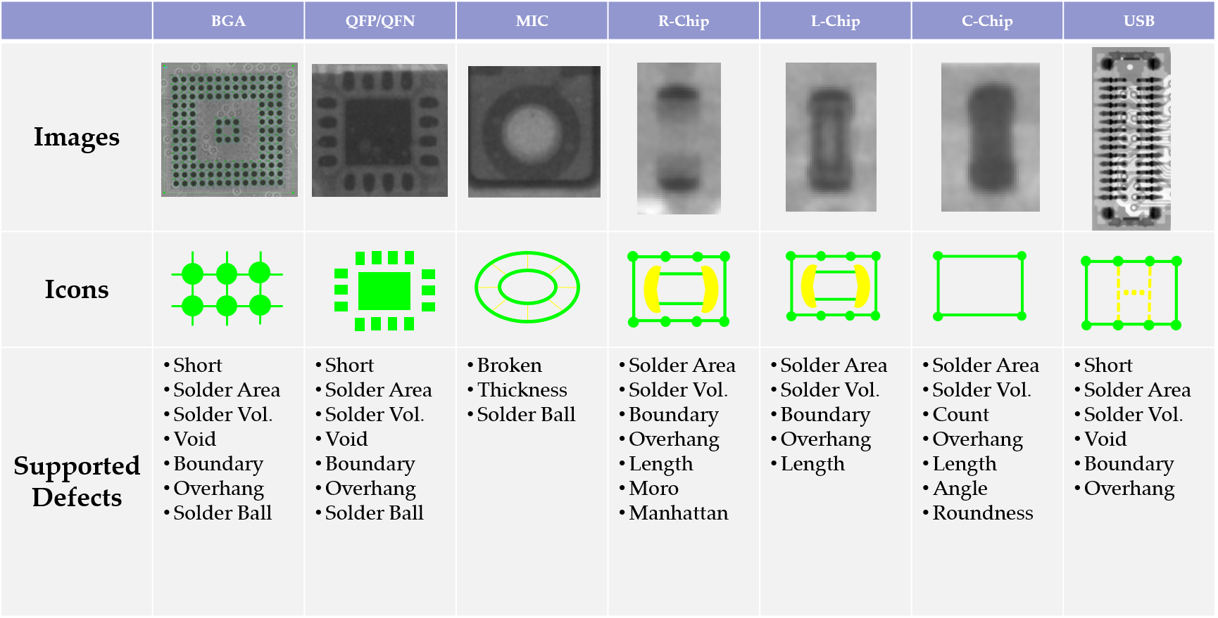
Review shorts, solder area, boundaries, overhang, length, angle, roundness, and other package-specific conditions
Use batch simulation and UDP communication to move from setup toward production integration
02 / CAPABILITIES
The HADI interface keeps image preparation, inspection regions, results, and supporting tools in one working environment
PCB INSPECTION
HADI-iBoard supports multiple component families, allowing the inspection logic to reflect the geometry and defect conditions that matter for each package
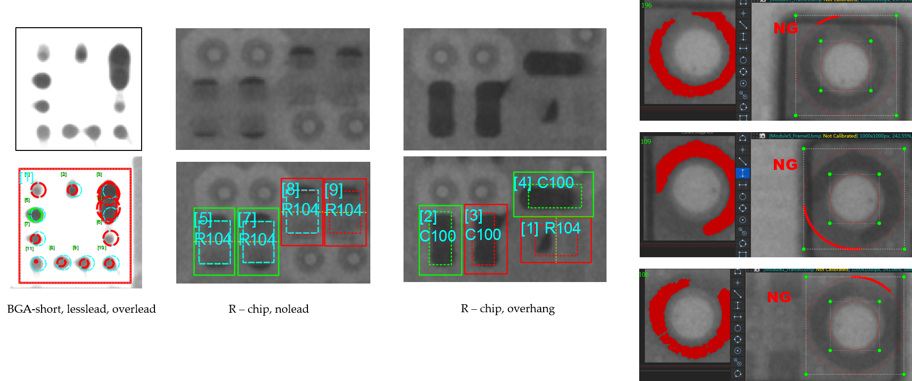
INSPECTION EXAMPLES
Taught regions and measurement rules turn component images into repeatable checks that can be reviewed and compared
LINE CONNECTION
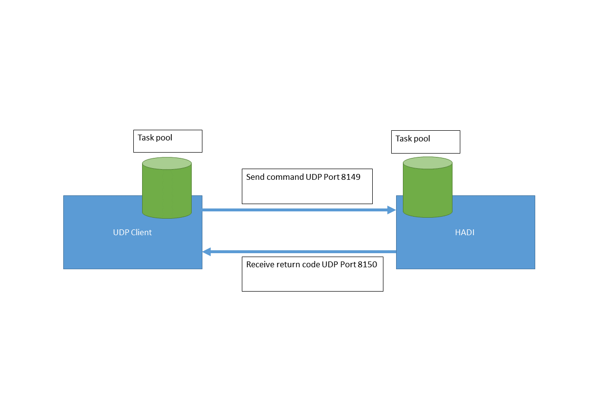
Use the same communication model as InspectionPro to receive an inspection command and return a result code to a third-party application
03 / WORKFLOW
Choose the component and inspection criteria
Build and validate the component template
Review the logic across multiple images
Exchange tasks with the wider inspection line
04 / SHARED HADI TOOLKIT
Every HADI product includes the foundational tools needed to load, prepare, measure, review, and communicate 2D X-ray images
SOFTWARE DOWNLOADS
Find archived installers, product manuals, and the industrial software guide in one library. Check the version and license requirements before changing a production workstation.
Open software downloads